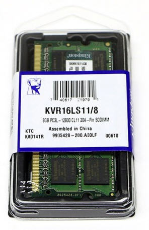
EDEC standard 1.35V (1.28V ~ 1.45V) and 1.5V (1.425V ~
1.575V) Power Supply
VDDQ = 1.35V (1.28V ~ 1.45V) and 1.5V (1.425V ~ 1.575V)
800MHz fCK for 1600Mb/sec/pin
8 independent internal bank
Programmable CAS Latency: 11, 10, 9, 8, 7, 6
Programmable Additive Latency: 0, CL – 2, or CL – 1 clock
8-bit pre-fetch
Burst Length: 8 (Interleave without any limit, sequential with starting address “000′ only), 4 with tCCD = 4 which does not allow seamless read or write [either on the fly using A12 or MRS]
Bi-directional Differential Data Strobe
Internal(self) calibration : Internal self calibration through ZQ pin (RZQ : 240 ohm ± 1%)
On Die Termination using ODT pin
Average Refresh Period 7.8us at lower than TCASE 85°C, 3.9us at 85°C < TCASE < 95°C Asynchronous Reset PCB: Height 1.18' (30mm), double sided component
| Weight | 0.03 kg |
|---|---|
| Dimensions | 42 × 78 × 4 cm |
Be the first to review “Product” Cancel reply
You must be logged in to post a review.
Related products
Product
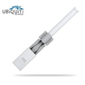
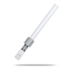
Ubiquiti 5GHz AirMax Dual Omni directional 10dBi Antenna – All mounting accessories and brackets included
Uncategorised
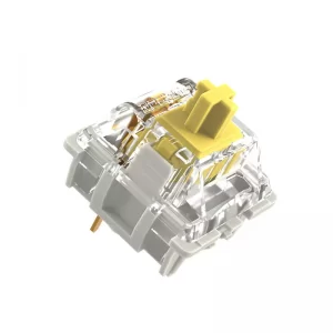
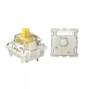
Gateron KS-9 G PRO Switches for Mechanical Gaming Keyboards | Plate Mounted | Pre Lubed (Gateron PRO Yellow, 1Pc)
Product
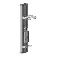
Ubiquiti High Gain 4.9-5.9GHz AirMax Base Station Sectorized Antenna 19dBi, 120 deg – All mounting accessories and brackets included
LENOVO V330 Extended Warranty: 1 Year to 3 Year Upgrade RTB (Virtual item) Please confirm with AM before purchase
Product
Ubiquiti 2GHz AirMax Dual Omni directional 10dBi Antenna – All mounting accessories and brackets included
Product
Verbatim 16GB V3 USB3.0 Green Store’n’Go V3; Rectractable USB Storage Drive Memory Stick








Reviews
There are no reviews yet.